Let's Teardown a Forty Quid Managed Switch - Part 2
Last time , we broke down the switch and had a look around its PCB. We identified some chips, found their datasheets, and learned a bit about how it's put together. This time let's get a bit more "hacky" and see if we can dump or decode anything.
Up front, you're going to have to excuse my soldering on this one. I've no idea what kind of solder or board process they used on this thing. Some of the through holes weren't really all-the-way-through holes, and no matter how much flux or fresh solder I laid down, this was as close to a clean joint as I got. I'm pretty sure if I spent any more time on it, I'd have lifted a pad or snapped a trace. I could clean it up with a splash of IPA and a scrub, but I'm going to reverse it all once I'm done anyway
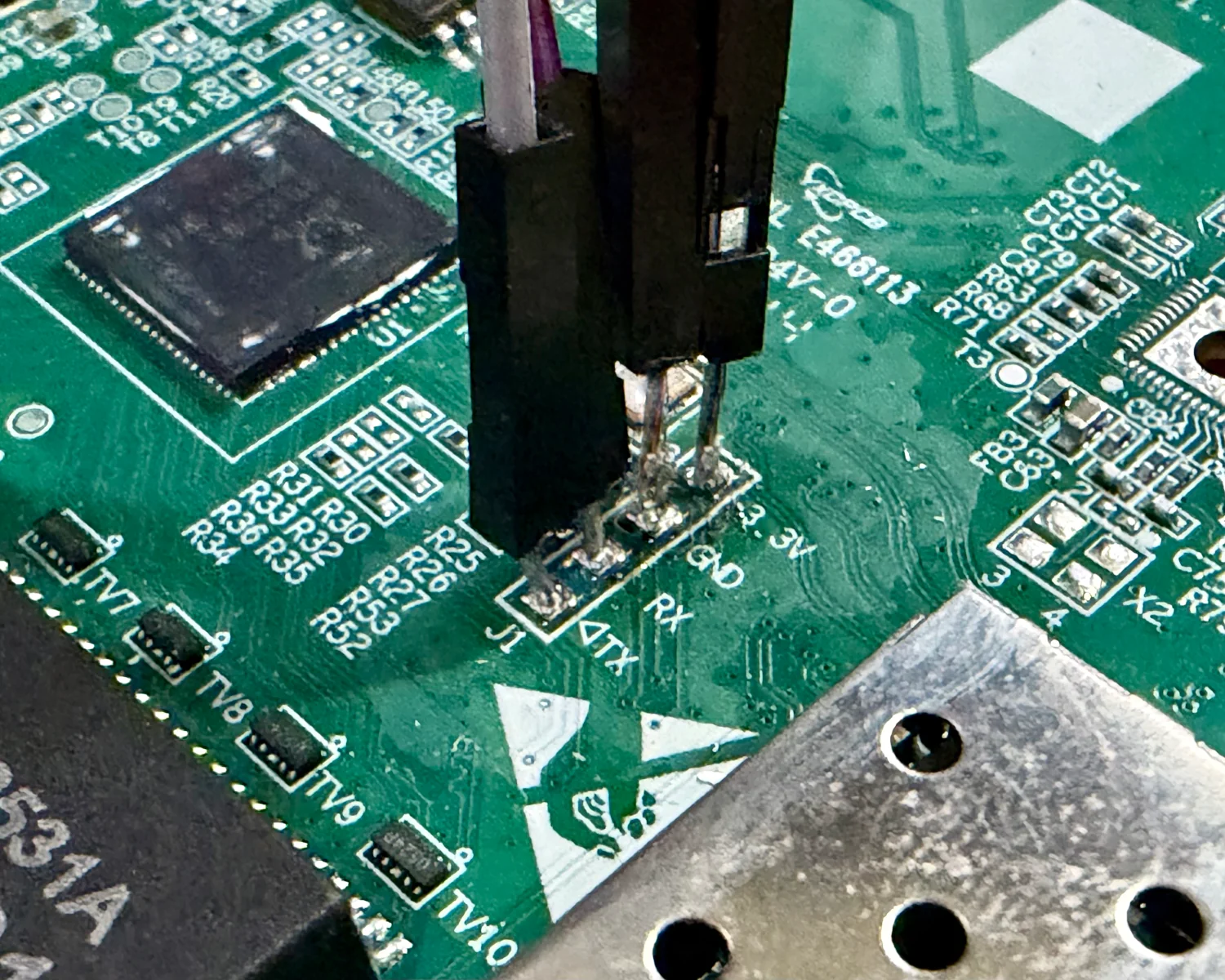
For the bulk of this post, I'm going to be sticking to pretty affordable tools. I'm going to be using a commonly available logic analyser and a very low-cost UART adaptor .
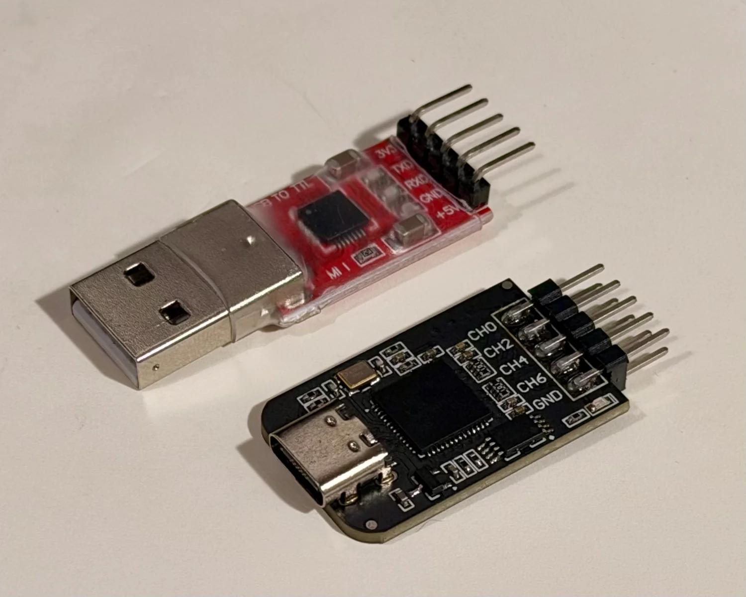
With the UART header soldered and the wires connected, we can connect the logic analyser. This will allow us to capture any messages the switch transmits on boot and attempt to decode them.
We're going to capture at ~1 MHz to ensure we get enough sample points on the signal to determine its baud rate. 1 G samples will give us 1000 seconds, or over 15 minutes, which is more than enough time to grab anything useful.
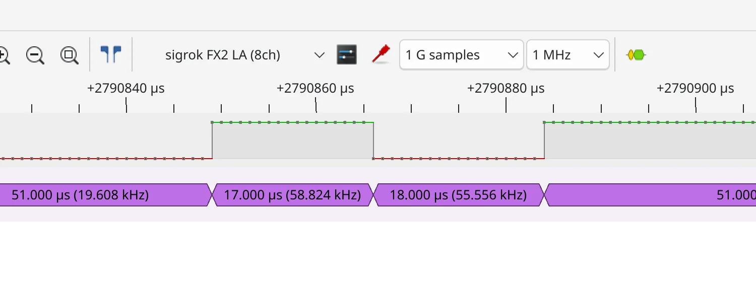
Adding a Timing decoder in PulseView, lets us see that a pulse is between 17 & 18 μs, with a calculated frequency of 55–59 kHz. Old-school nerds might remember the glory days of UARTs and serial ports; 9600 bps, 57600 bps, and 115200 bps were all common. The baud rate of 57,600 bps is equal to ~17.36 μs, which is pretty much bang-on what we're seeing.
Turning to PulseView's UART decoder, we can tell it to treat our capture as a 57,600 bps UART signal and decode the bytes as ASCII.
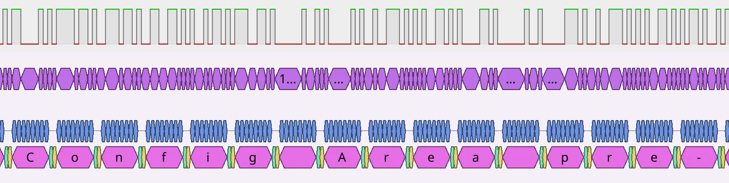
We can see real, live ASCII data flowing from the UART pins on the switch. Bingo!
Switching from the analyser to the UART adaptor, we can run
tio
and see what the switch is telling us.
==========Loader start V0.2===========
Press any key to start the normal procedure.
To run SPI flash viewer, press [v]
To enforce the download of the runtime kernel, press [ESC] .....
  cmd -1
    Check Runtime Image.....
    Chksum Correct!
    RunTime Kernel Starting....
Ver8372N=2
Ver8373N=2
LINE 1472, RL6818C_pwr_on_patch_phy_v007 , patch 0xf0 finished!


===========================Config Area pre-check Starts.=====================.
Pre-Check the config size structure is equal or not.
It seems no risk!..................
==============================Config Area pre-check ends.===================.


SalFlshCopyFlshToCache()
sal_sys_config_restore()
Restore dhcp state is: 0

Restore ip is: 192.168.2.1

...OK
sal_mirror_config_restore()...OK
sal_qos_config_restore()...OK
sal_vlan_config_restore()...OK
sal_rate_config_restore()...OK
sal_trunk_config_restore()...OK
sal_l2_config_restore()...OK
sal_loop_config_restore()...OK
sal_eee_config_restore()...OK
sal_stp_config_restore()...OK
sal_igmp_config_restore()...OK
sal_dhcp_snooping_config_restore()...OK
sal_port_config_restore()...OK

################################################################

############Login Menu ############
### Please input uboot password below: ###
Now, despite my best efforts, none of the usual suspects work here. No matter what I tried, I couldn't brute force this password by hand.
We were given a few hints for some other menus that might be available to us. The first one to try is "Esc".
==========Loader start V0.2===========
Press any key to start the normal procedure.
To run SPI flash viewer, press [v]
To enforce the download of the runtime kernel, press [ESC] .....
  cmd 27
sal_sys_runtime_crc_set
loader start
Ver8372N=2
Ver8373N=2
LINE 1462, RL6818C_pwr_on_patch_phy_v007 , patch 0xf0 finished!
load MAC from nvcfg
  IP:192.168.1.1
Mask:255.255.255.0
  GW:192.168.1.254
 MAC:1C.2A.A3.31.C2.61
This seems to be some sort of "unbrick" menu.
That IP address isn't the normal default IP; the switch normally boots up to 192.168.
2
.1.
It might be worth running a quick
nmap
scan when the switch is in this mode to see what's running.
I wonder if there's a TFTP server here, or something?
There are no other screens or menus here, so let's reboot the switch and try the "SPI flash viewer" from the "v" option.
==========Loader start V0.2===========
Press any key to start the normal procedure.
To run SPI flash viewer, press [v]
To enforce the download of the runtime kernel, press [ESC] ..
=========================SPI FLASH VIEWER=============================
    b: reboot
    e <addr>: Erase flash with the address of <addr>
    ev <addr>: Erase flash with the address of <addr> and then Verify
    r <addr> <len>: read flash from the address of <addr> and then dump
    c: check runtime kernel without boot
    cb: check runtime kernel and boot if checksum is pass
    h: print header
    l: load runtime kernel
    v: show verobose information
    m: print this menu
    q: quit from spi flash view
>
Right, there are a lot of options here. Let's go through some of them.
"c", "h", and "v" all seem to show some data about the firmware, but nothing too exciting.
>c
    Chksum Correct!
>h
    magic_number:  0x12345678
    length:        0x000e3318 (930584)
    header_chksum: 0x000003fc
    payload_chksum:0x047f293a
    reserved:      0x332255ff
>v
There 2 protected region(s).
    Portected region 0: 0x000000-0x001000
    Portected region 1: 0x004000-0x01c000
>
"r" is much more interesting. We can use this to read areas from the flash chip. Here's what the first 256 bytes look like.
>r 0x0 0xff
         00 01 02 03 04 05 06 07 08 09 0A 0B 0C 0D 0E 0F
[000000] 00 40 02 0c e7 ef c3 60 01 d3 92 00 22 02 0e 40  .@.....`...."..@
[000010] 8f 96 22 00 00 02 0e d8 90 1c c2 12 08 ab e4 fe  ..".............
[000020] ff 22 00 00 00 02 0d ac 90 16 b6 12 08 ab e4 ff  ."..............
[000030] fe fd fc 90 16 ba 12 08 ab c0 96 75 96 03 e4 ff  ...........u....
[000040] 7e c0 fd fc 90 16 b6 12 08 41 c3 12 07 9e 50 03  ~........A....P.
[000050] 02 00 b1 e4 fc fd fe 90 40 00 e4 f8 f9 fa e4 93  ........@.......
[000060] 28 f8 e4 39 f9 a3 da f6 e8 2c fc e9 3d fd e4 3e  (..9.....,..=..>
[000070] fe e5 83 70 e5 90 16 bd e0 2c f0 90 16 bc e0 3d  ...p.....,.....=
[000080] f0 90 16 bb e0 3e f0 90 16 ba e0 34 00 f0 e5 96  .....>.....4....
[000090] 04 f5 96 90 16 b6 12 08 25 c3 ef 94 00 ff ee 94  ........%.......
[0000a0] c0 fe ed 94 00 fd ec 94 00 fc 90 16 b6 12 08 ab  ................
[0000b0] 02 00 3c 90 16 b8 e0 f9 a3 e0 f8 90 16 ba e0 ff  ..<.............
[0000c0] a3 e0 fe a3 e0 fd a3 e0 fc 90 40 00 e8 49 60 15  ..........@..I`.
[0000d0] 18 b8 ff 01 19 e4 93 2c fc e4 3d fd e4 3e fe e4  .......,..=..>..
[0000e0] 3f ff a3 80 e7 90 16 ba ef f0 a3 ee f0 a3 ed f0  ?...............
[0000f0] a3 ec f0 d0 96 90 16 ba 12 08 25 22 00 00 00 00  ..........%"....
length=0x100(256).
>
00 40 02 0c e7 ef c3 60
through to
12 08 25 22 00 00 00 00
.
Now we've explored everything we can easily get to through the UART; it's probably time to start looking at the firmware itself. You could likely use that "r" command to read back the whole flash chip and then write a short script to convert the hex into a binary file. That all sounds a little too much like work for me, though. What if we could read the flash chip directly and pull the firmware out?
Luckily, we can "attack" the flash chip itself with a "chip clip" connected to my trusty Glasgow Interface Explorer .
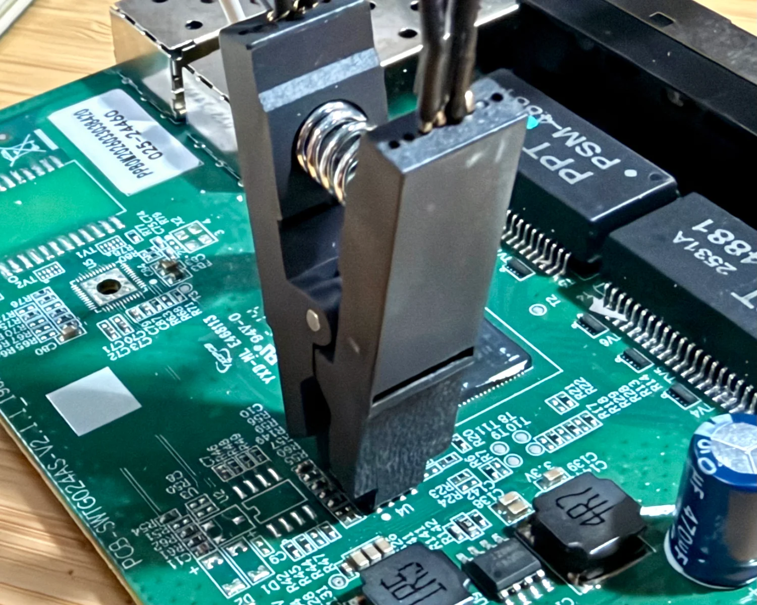
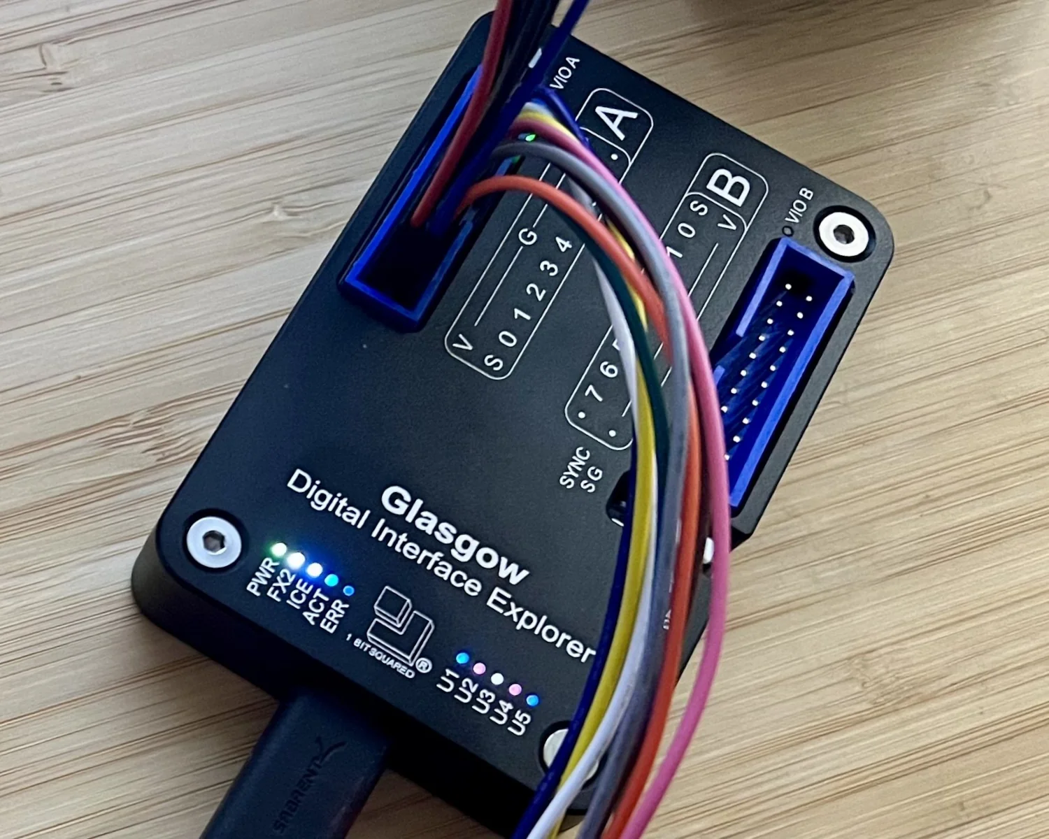
It takes a bit of squinting, but this chip's code reads 25Q16JVSN.
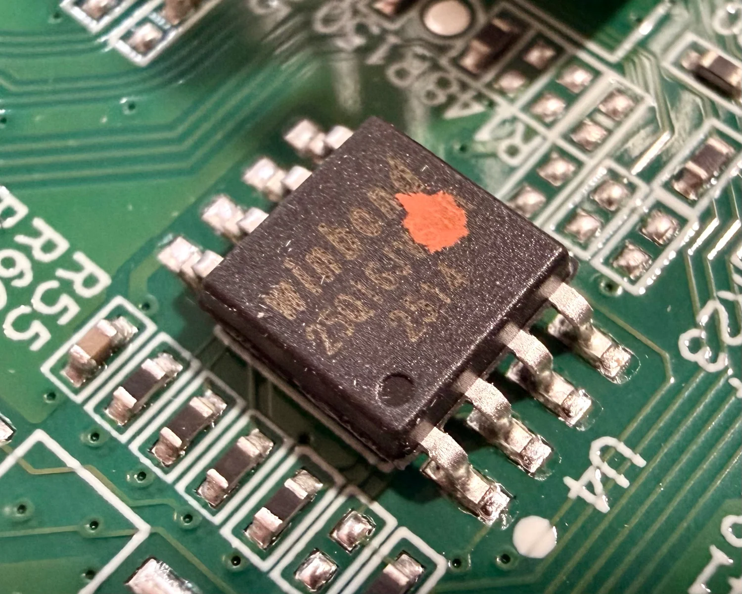
Referring to the datasheet , we can tell it's a 25Q chip, with 16M-bit of space, running at 3.3 V (more properly, 2.7–3.6 V), in an SO8 package. The Glasgow is distributed with an applet that can read 25Q compatible chips, so we can ask it to dump the "first" 2097152, or (16 ÷ 8) × 1024 × 1024, bytes.
mike@framework ~> glasgow run memory-25q -V 3.3 read -f firmware.dump 0 2097152
I: g.hardware.device: device already has bitstream ID aa65dda7f1023326
I: g.hardware.assembly: port * voltage set to 3.3 V
I: g.cli: running handler for applet 'memory-25q'
W: g.a.memory.25q: device does not have valid SFDP tables: SFDP signature not present
W: g.a.memory.25q: assuming --address-bytes 3 by default
reading: 100%|██████████████████████████████████████████████| 2.0Mi/2.0Mi [00:02<00:00, 1.45MB/s]
mike@framework ~>
We can then get Glasgow to verify the dump by reading it out a second time and comparing results.
mike@framework ~> glasgow run memory-25q -V 3.3 verify -f firmware.dump 0
I: g.hardware.device: device already has bitstream ID aa65dda7f1023326
I: g.hardware.assembly: port * voltage set to 3.3 V
I: g.cli: running handler for applet 'memory-25q'
W: g.a.memory.25q: device does not have valid SFDP tables: SFDP signature not present
W: g.a.memory.25q: assuming --address-bytes 3 by default
reading: 100%|██████████████████████████████████████████████| 2.0Mi/2.0Mi [00:02<00:00, 1.45MB/s]
I: g.a.memory.25q: verify PASS
mike@framework ~>
Success!
Now, let's take a quick peek at the first 256 bytes of the dump, using
xxd
.
mike@framework ~> xxd -c 16 -l 256  two-meg.dump
00000000: 0040 020c e7ef c360 01d3 9200 2202 0e40  .@.....`...."..@
00000010: 8f96 2200 0002 0ed8 901c c212 08ab e4fe  ..".............
00000020: ff22 0000 0002 0dac 9016 b612 08ab e4ff  ."..............
00000030: fefd fc90 16ba 1208 abc0 9675 9603 e4ff  ...........u....
00000040: 7ec0 fdfc 9016 b612 0841 c312 079e 5003  ~........A....P.
00000050: 0200 b1e4 fcfd fe90 4000 e4f8 f9fa e493  ........@.......
00000060: 28f8 e439 f9a3 daf6 e82c fce9 3dfd e43e  (..9.....,..=..>
00000070: fee5 8370 e590 16bd e02c f090 16bc e03d  ...p.....,.....=
00000080: f090 16bb e03e f090 16ba e034 00f0 e596  .....>.....4....
00000090: 04f5 9690 16b6 1208 25c3 ef94 00ff ee94  ........%.......
000000a0: c0fe ed94 00fd ec94 00fc 9016 b612 08ab  ................
000000b0: 0200 3c90 16b8 e0f9 a3e0 f890 16ba e0ff  ..<.............
000000c0: a3e0 fea3 e0fd a3e0 fc90 4000 e849 6015  ..........@..I`.
000000d0: 18b8 ff01 19e4 932c fce4 3dfd e43e fee4  .......,..=..>..
000000e0: 3fff a380 e790 16ba eff0 a3ee f0a3 edf0  ?...............
000000f0: a3ec f0d0 9690 16ba 1208 2522 0000 0000  ..........%"....
mike@framework ~>
It's reassuring that this excerpt from the dump exactly matches the section we read out over UART earlier.
0040 020c e7ef c360
to
1208 2522 0000 0000
.
With a dumped blob in hand, it's time to start analysing and reverse engineering the firmware; but that's for another day.
2026-10-16